Xyloni開発キットへの書き込み
作成者:mou-mou
先日、Xyloni®開発キット チュートリアルの実践を行い、チュートリアルの資料だけではデバイスへの書き込み部分がわかりにくかったのでまとめてみました。
デバイスドライバの切り替え
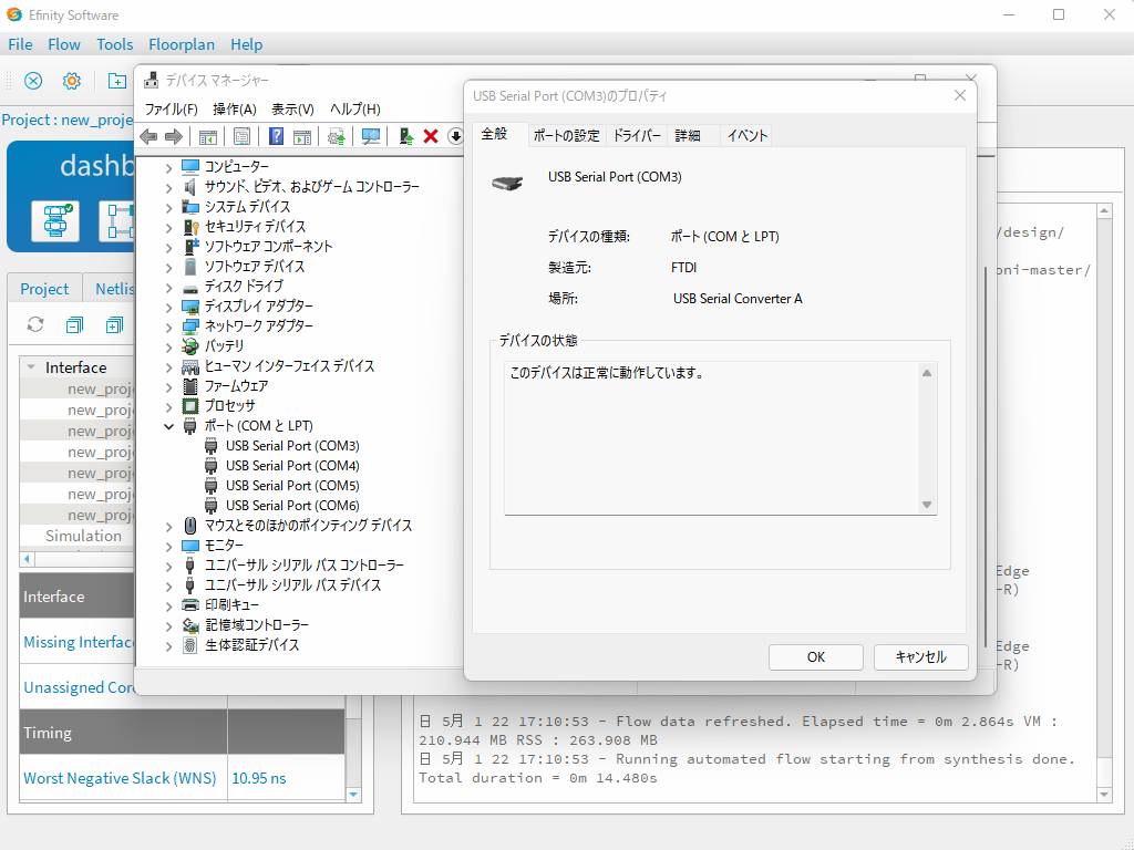
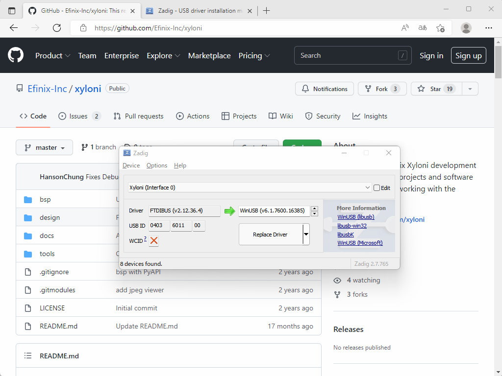
XyloniをPCにUSBケーブルで接続します。そしてデバイスマネージャでUSBデバイスの認識を確認します。そうすると、FT4232Hが搭載されている為、4つのCOMポートが見えます。
| Interface 0 | SPI ( Flash Memory / FPGA) |
| Interface 1 | JTAG |
| Interface 2 | UART通信 |
| Interface 3 | VCCIO選択 |
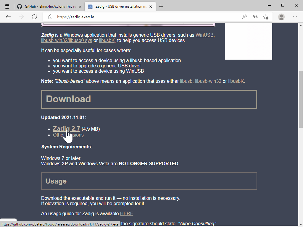
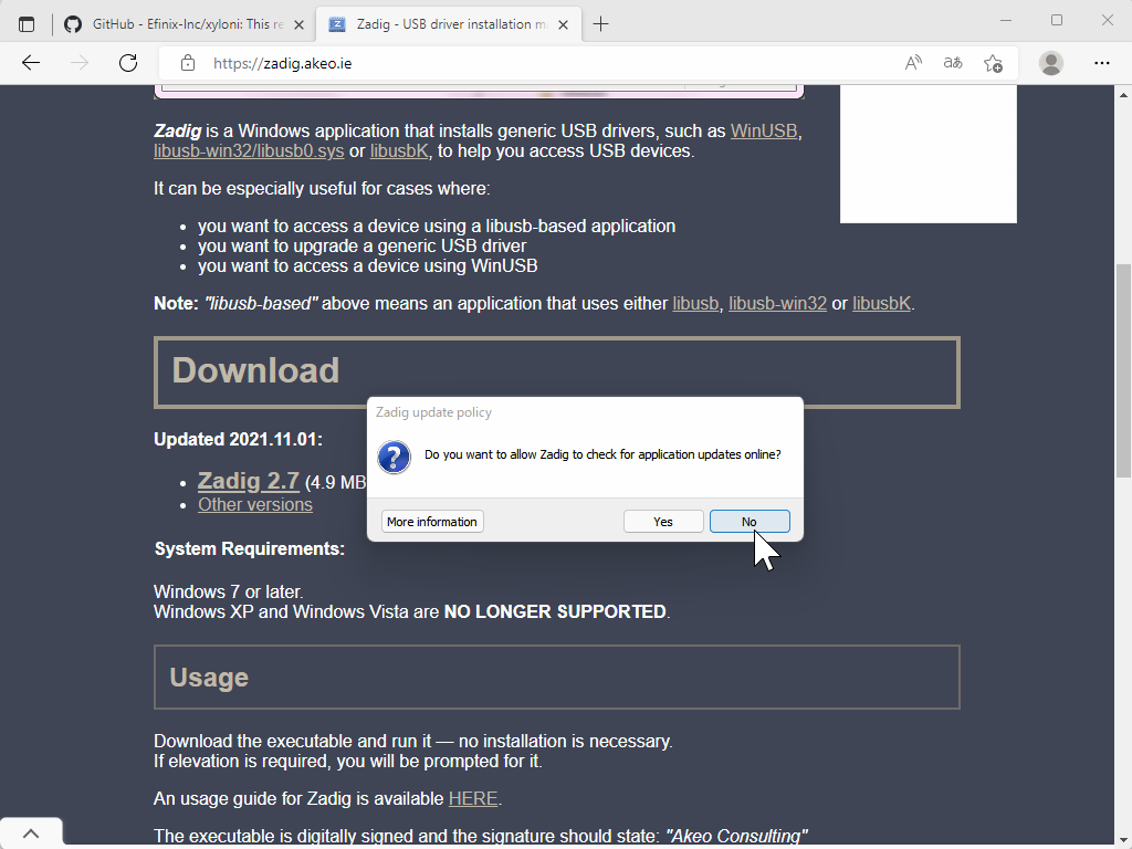
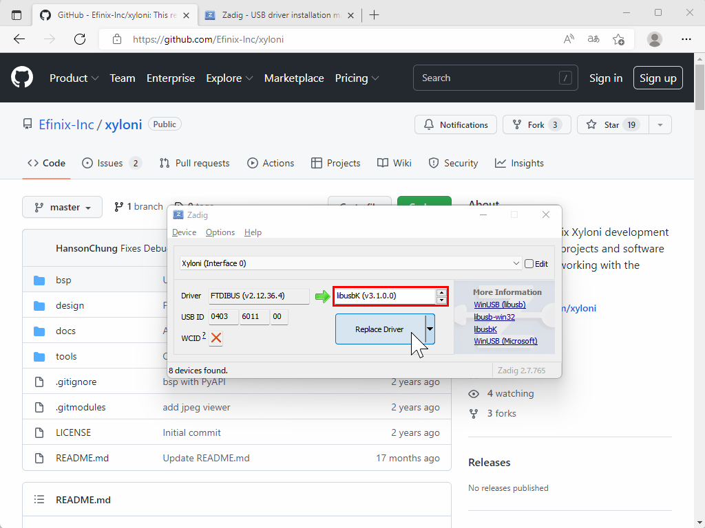
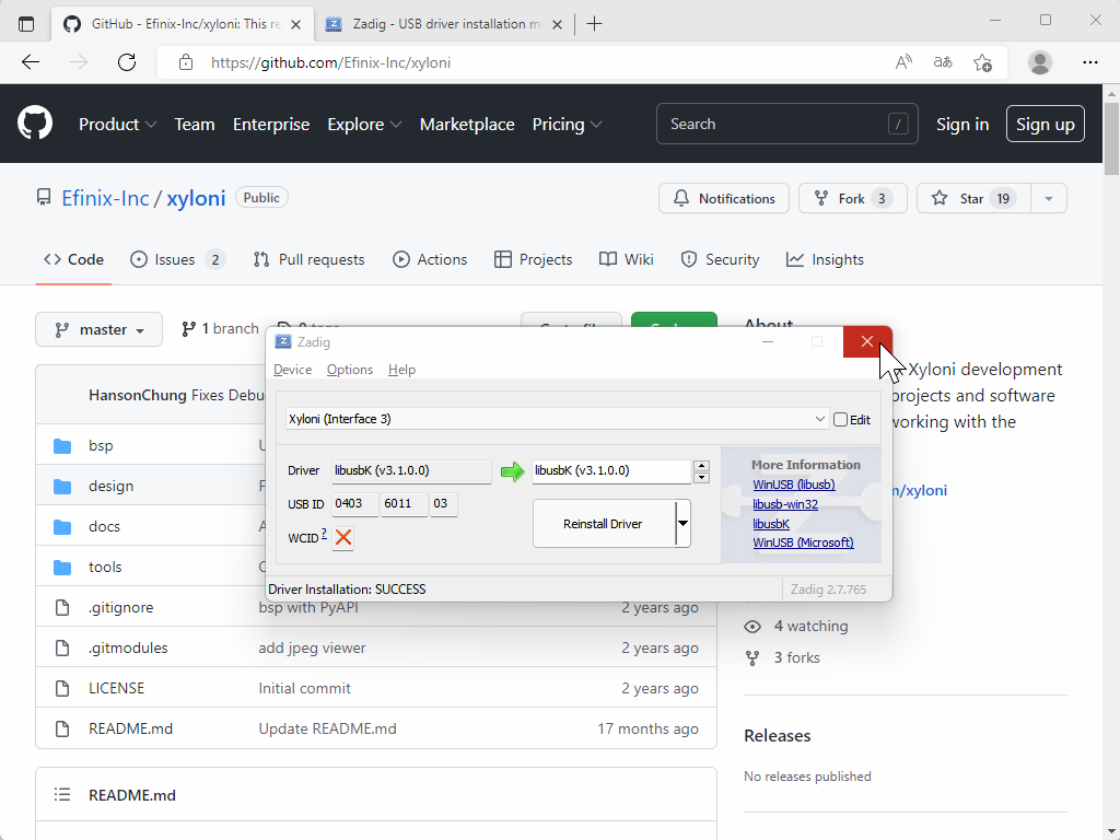
デバイスドライバの切り替えのために、Zadigをダウンロードします。
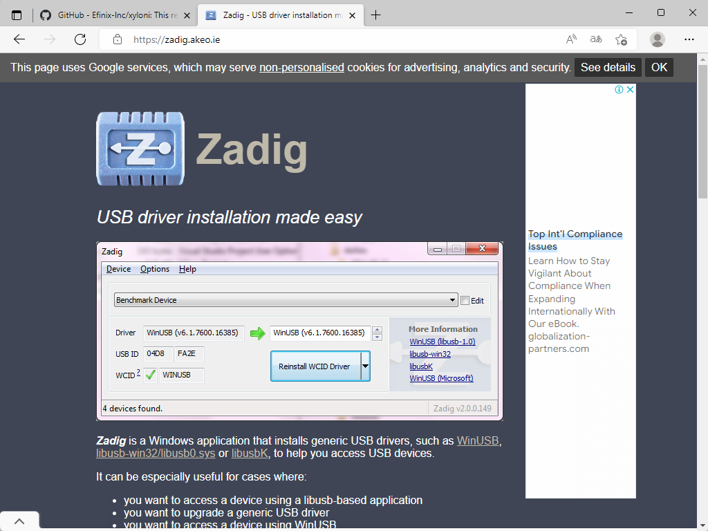
Zadigを起動します。
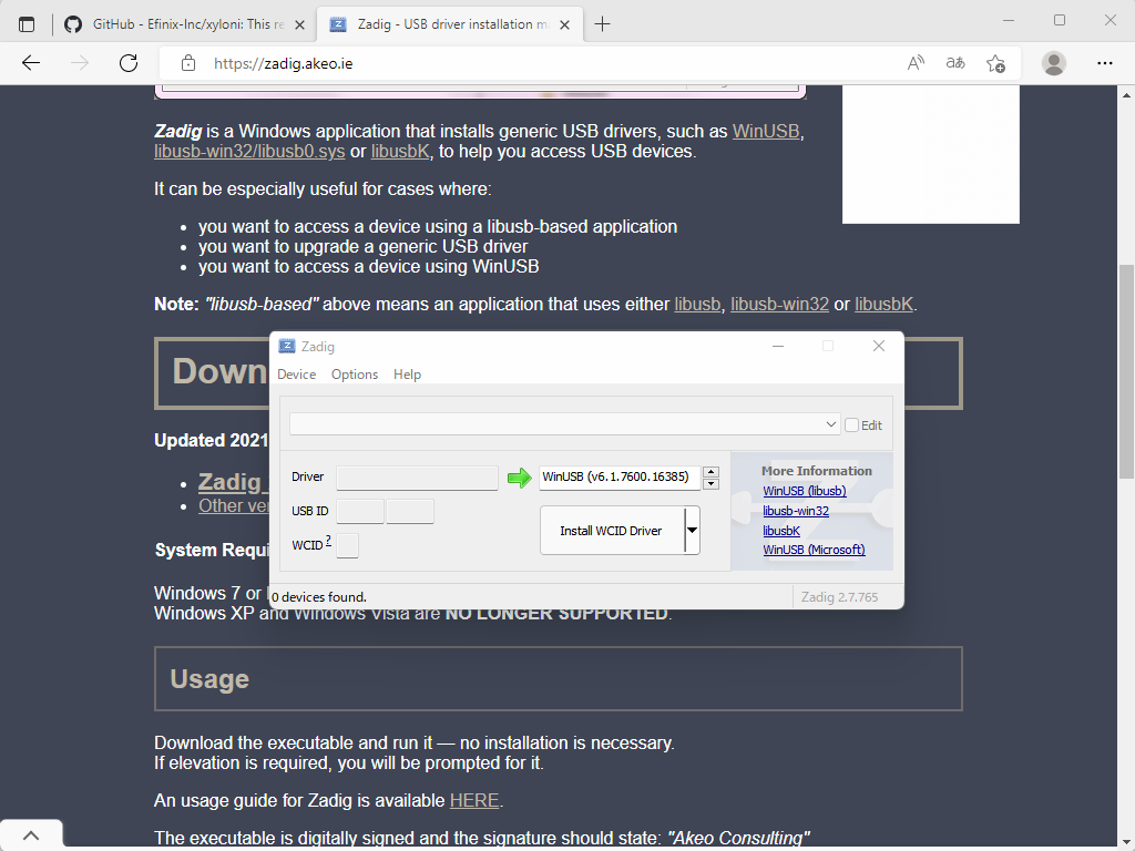
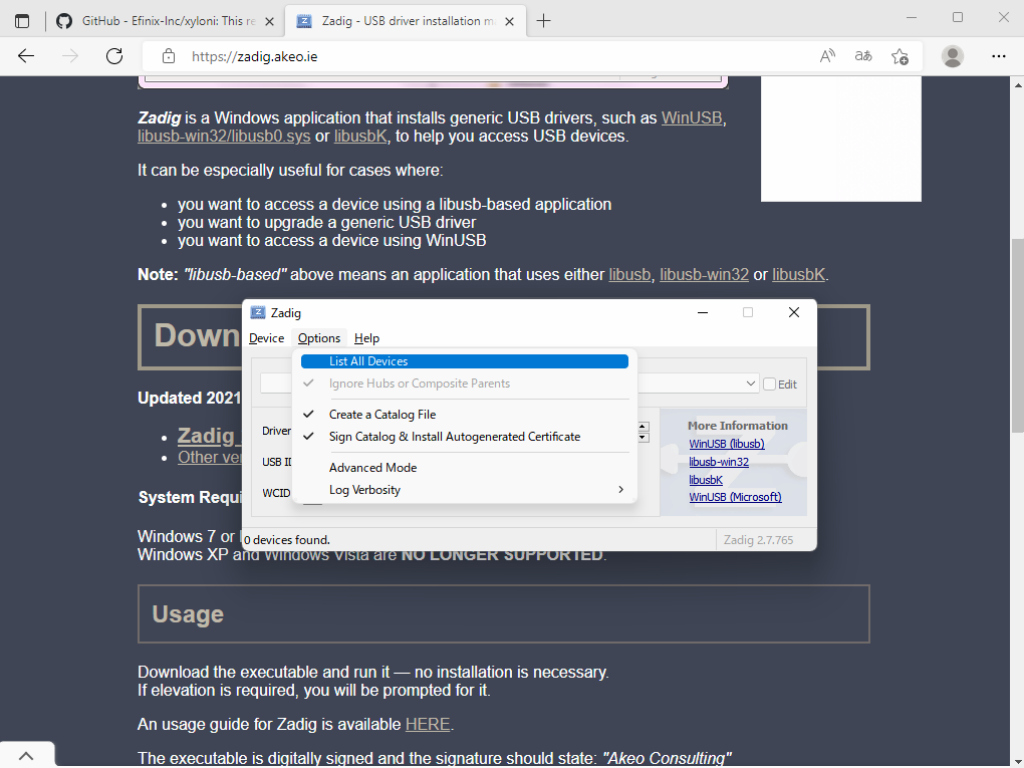
すべてのデバイスリストを取得します。
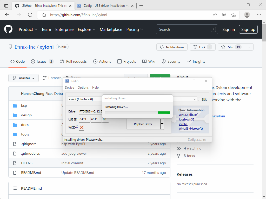
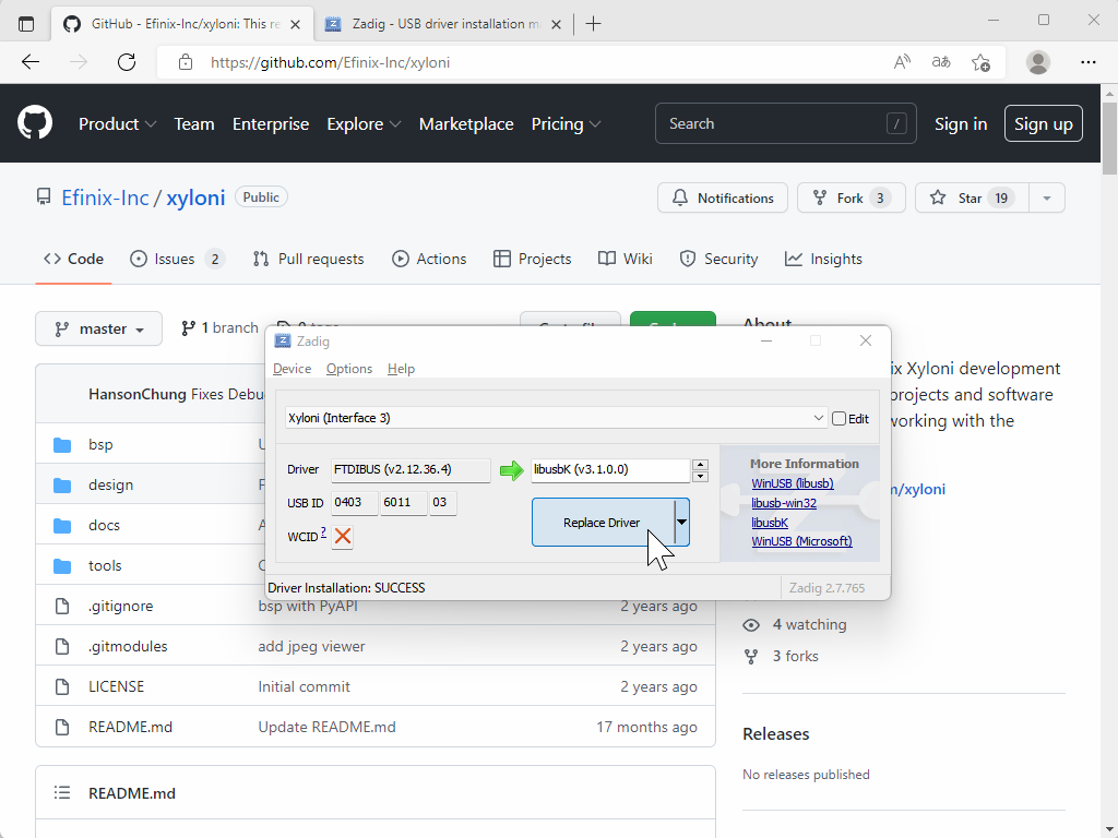
Xyloni (interface 0), Xyloni (interface 1), Xyloni (interface 3)をFTDIBUSからlibusbkに変更していきます。
Xyloni (interface 2)は、UART通信に使用しするので、変更してはなりません。


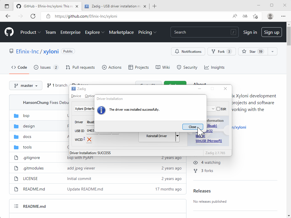

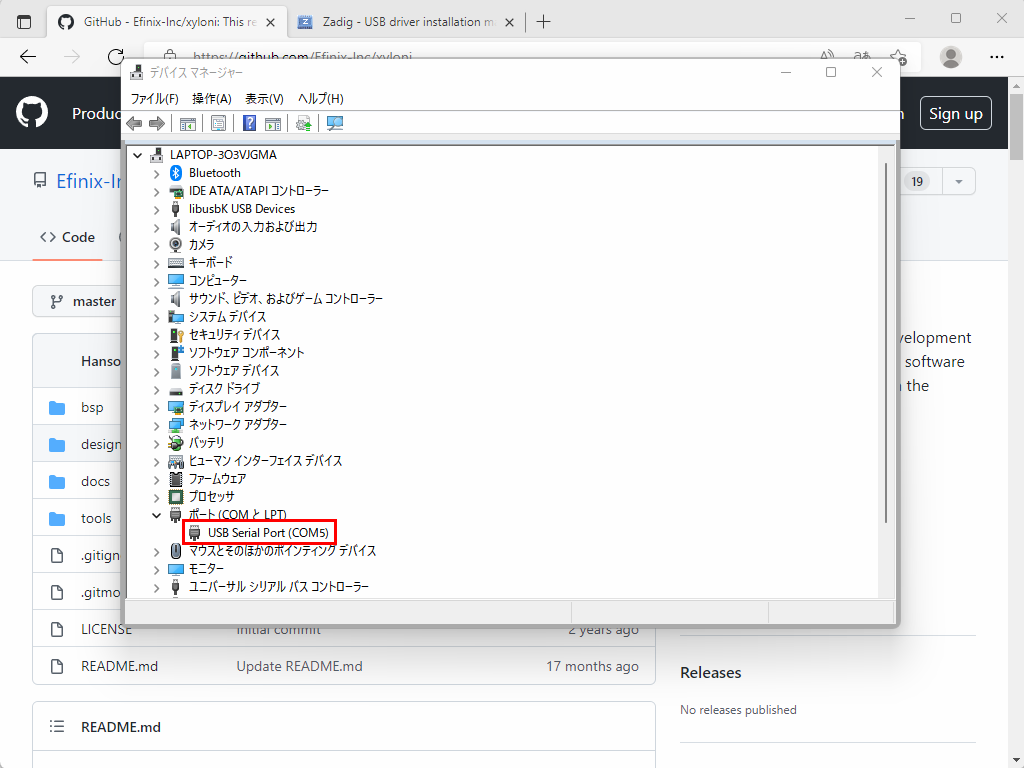
もう一度デバイスマネージャで確認すると、COMポートは1つになっています。
書き込み
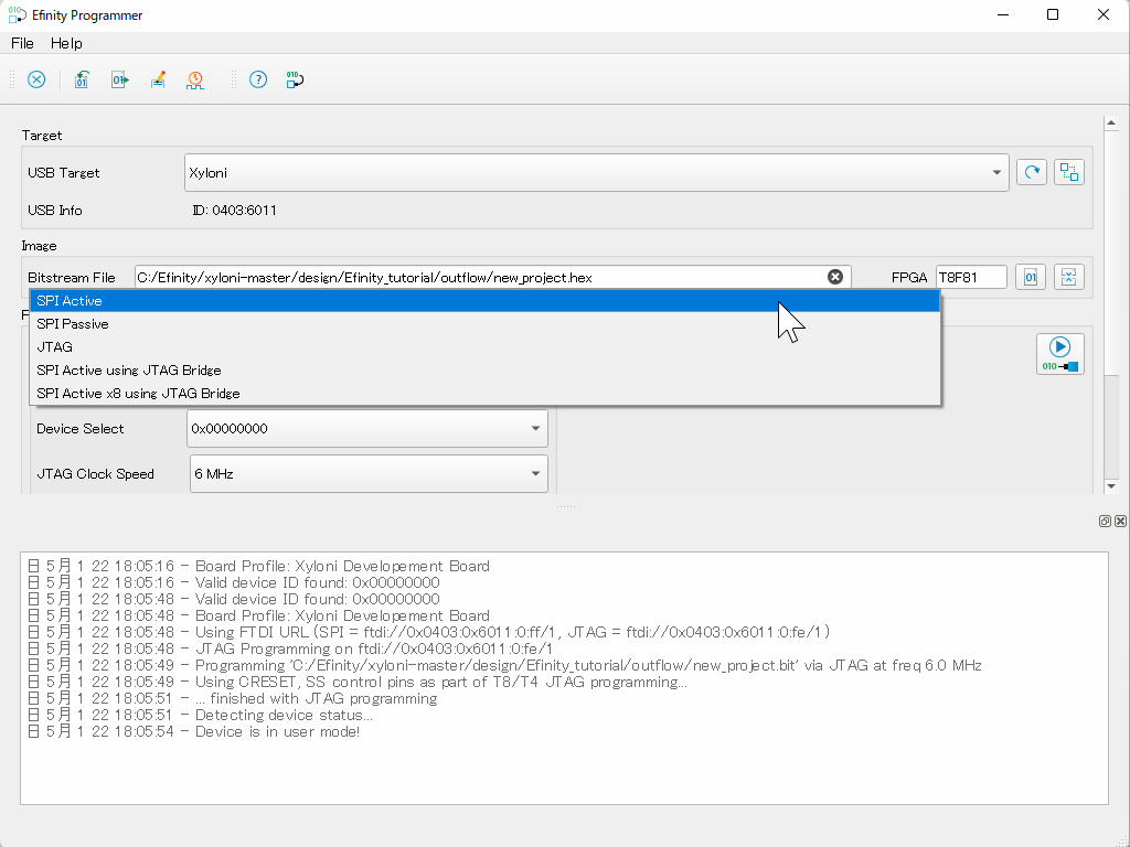
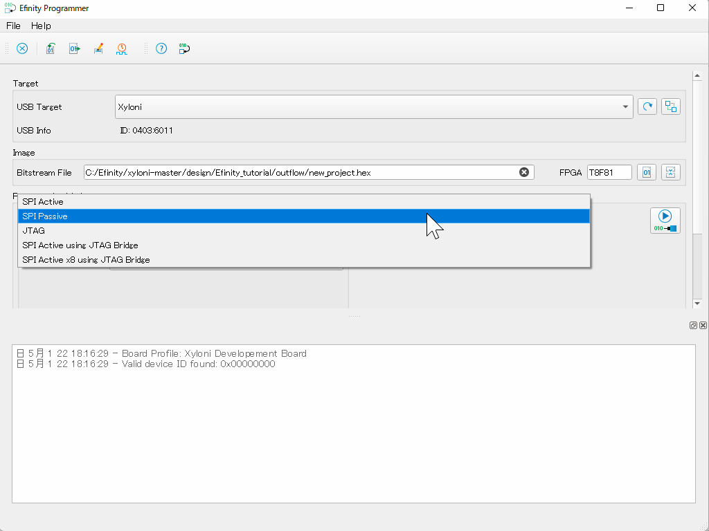
書き込みには、4種類の方法があります。
| SPI Active | オンボードのFLASHメモリにSPIで書き込み |
| SPI Passive | FPGAにSPIで書き込み(RAMへ書き込み) |
| JTAG | FPGAにJTAGで書き込み(RAMへ書き込み) |
| SPI Active using JTAG | JTAGでFPGAを介してFLASHメモリに書き込み |
評価ボードでは、SPIとJTAG両方がFT4232Hに接続されている為、デバッグもFlash書き込みも出来ます。製品版のボードを開発する場合は、コスト面やスペースの問題で2種類のインタフェースを用意したくない場合に、SPI active using JTAGを使用して、JTAGからFPGAを介してFLASHメモリに書き込みを行います。専用のFPGAイメージを用意したり少し手間かかりますので、別の機会にご紹介できればと思っております。
JTAG 書き込み
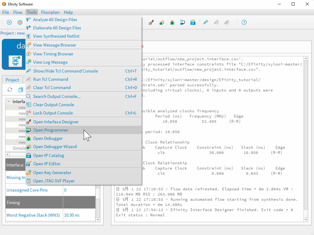
プログラマを起動します。

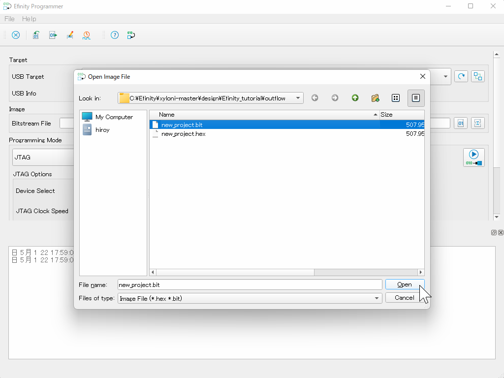
書き込むイメージファイルを選択します。
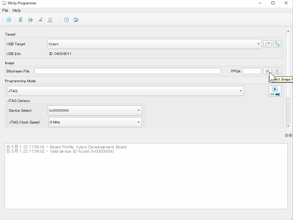
JTAG書き込みでは、bitファイルを選択します。
書き込みを実行します。

SPI Active
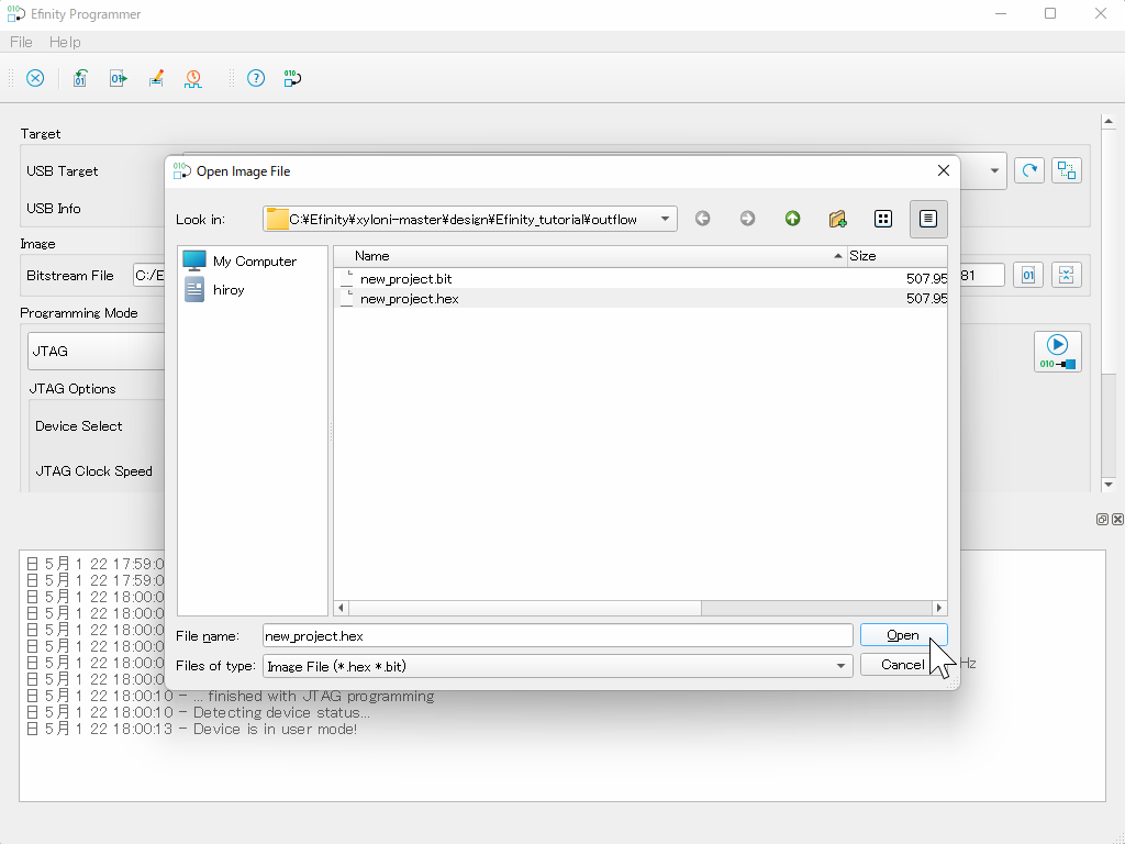
SPI Active書き込みでは、hexファイルを選択します。
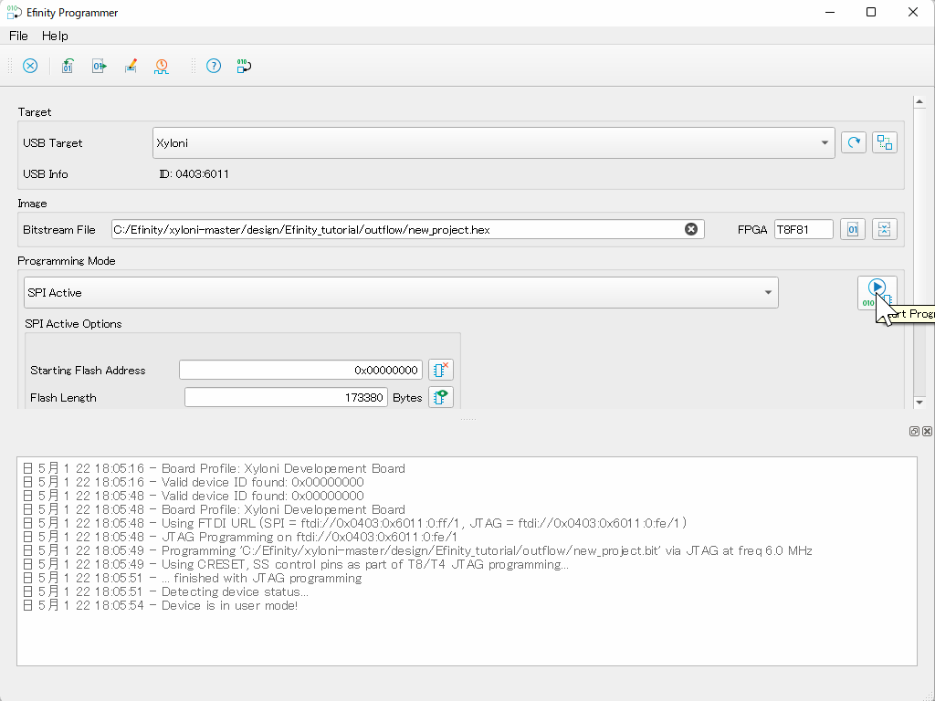
書き込みモードをSPI Activeにします。
書き込みを実行します。
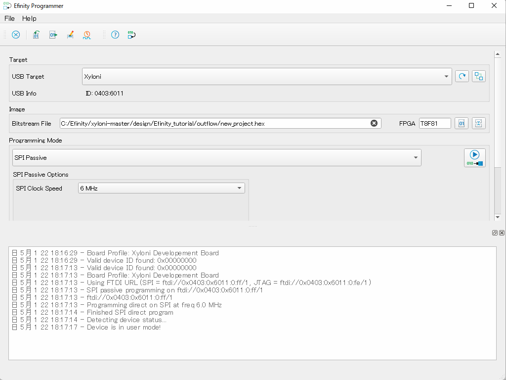
SPI Passive
書き込みモードをSPI Passiveにします。
ファイルは既にhexを選択している為、そのまま書き込みを実行します。